SCHOTT multilayer ceramics optimize surface-mount packages for RF applications

Hermetic hybrid housings improve signal path quality and allow for high-density packaging

Landshut (Germany) & Grenoble (France), September 9, 2013 – The international technology company SCHOTT offers high performance miniaturized hermetic hybrid housings with a bandwidth greater 30 GHz. By using multilayer ceramic feedthroughs, they bridge the height difference between the RF signal inside a surface-mount device and the host board. SCHOTT uses virtual prototyping to achieve the optimal design quickly and efficiently. SCHOTT is showcasing its hybrid housings at the European Microelectronics and Packaging Conference in Grenoble, France (September 9-12, 2013, Booth 45).

Sensitive optoelectronic components used in the high-speed data and telecommunication industries, especially in the radio frequency (RF) range, require reliable protection in a harsh environment. Increasing miniaturization adds to the challenging requirements of customizing packaging designs. That is why SCHOTT resorts to sophisticated multilayer ceramic structures to solve interconnection problems in high-density packaging.

Used as hermetic feedthroughs, multilayer ceramics are ideal to bridge the height difference of the planar waveguide for the signal path inside the housing and the host board, while keeping the RF path reflection at a minimal level. They also allow for complex structures of electrical, optical, and thermal interfaces to be integrated into the housing. Common butterfly packages, on the contrary, required cut-outs in the host board or bent leads – options, which for technical, design and assembly reasons were not ideal.

Designing compactness

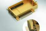
“Multilayer ceramics are well-suited for compact systems in high frequency applications,” says Robert Hettler, Head of R&D Opto-Electronics at SCHOTT Electronic Packaging. “They allow for connecting a high number of conductors to create a dense routing inside a hermetically sealed unit,” Hettler adds. To realize this unit, metallic lines and vias are applied to thin sheets of ceramic with the help of punching processes and silk screen printing. Several layers are then stacked, laminated and co-fired at high temperatures. A device is formed that can be mounted on the surface of a printed circuit board (PCB).

Recently, SCHOTT developed a space-saving, standard-looking surface-mount device with a bandwidth greater 30 GHz allowing for a highly customizable design of the package interior. Using Finite Element simulation tools to analyze the electromagnetic field, SCHOTT is able to model the most suitable packaging. The signal path quality can thus be improved before a prototype is actually created; shortening the time-to-market and enabling enhanced designs of hermetic hybrid packages.

Additional information: http://www.schott.com/epackaging /

Download link to a ZIP file that contains this picture in print quality:
http://www.schott-pictures.net/presskit/210943.empc2013 /, More press photographs available here: http://www.schott-pictures.net/

SMD RF package with 4 differential line pairs, each allowing for a data flux of up to 28 Gbit/s in the shown example. Source: SCHOTT

Download image

Electronic Packaging, as a business unit of the international technology group SCHOTT, is a leading manufacturer of housings and other components for the reliable, long-term protection for sensitive electronics. The core technologies are glass-to-metal and ceramic-to-metal sealing (LTCC and HTCC, Low and High Temperature Co-fired Ceramics), thermal sensing components as well as a variety of cutting edge specialty glass competences. With 1,500 employees at five production locations and several competence centers around the world, local customer support and co-developments for individual packaging solutions are at the heart of the business, serving the world’s leading manufacturers in the automotive, data- and telecommunication, sensors and semiconductors, consumer electronics, dental care, home appliances, laser as well as security and tracking industries.

SCHOTT is an international technology group with more than 125 years of experience in the areas of specialty glasses and materials and advanced technologies. SCHOTT ranks number one in the world with many of its products. Its core markets are the household appliance, pharmaceuticals, electronics, optics, solar power, transportation and architecture industries. The company is strongly committed to contributing to its customers’ success and making SCHOTT an important part of people’s lives with its high-quality products and intelligent solutions. SCHOTT is committed to managing its business in a sustainable manner and supporting its employees, society and the environment. The SCHOTT Group maintains close proximity to its customers with manufacturing and sales units in 35 different countries. Its workforce of around 16,000 employees generated worldwide sales of approximately 2 billion euros for the 2011/2012 fiscal year. SCHOTT AG, with its headquarters in Mainz, Germany, is owned by the Carl Zeiss Foundation.